D a t a S h e e t , R e v . 2 . 2 , A p r i l 2 00 8
B G A 6 22
Silicon Germanium Wide Band Low Noise
A m p l i f i e r w i t h 2 k V E S D P r o te c t i o n
S m a l l S i g n a l D i s c r et e s
�Edition 2008-04-14
Published by Infineon Technologies AG,
81726 München, Germany
© Infineon Technologies AG 2008.
All Rights Reserved.
Attention please!
The information herein is given to describe certain components and shall not be considered as a guarantee of
characteristics.
Terms of delivery and rights to technical change reserved.
We hereby disclaim any and all warranties, including but not limited to warranties of non-infringement, regarding
circuits, descriptions and charts stated herein.
Information
For further information on technology, delivery terms and conditions and prices please contact your nearest
Infineon Technologies Office (www.infineon.com).
Warnings
Due to technical requirements components may contain dangerous substances. For information on the types in
question please contact your nearest Infineon Technologies Office.
Infineon Technologies Components may only be used in life-support devices or systems with the express written
approval of Infineon Technologies, if a failure of such components can reasonably be expected to cause the failure
of that life-support device or system, or to affect the safety or effectiveness of that device or system. Life support
devices or systems are intended to be implanted in the human body, or to support and/or maintain and sustain
and/or protect human life. If they fail, it is reasonable to assume that the health of the user or other persons may
be endangered.
�BGA622
BGA622, Silicon Germanium Wide Band Low Noise Amplifier with 2 kV ESD Protection
Revision History: 2008-04-14, Rev. 2.2
Previous Version: 2005-11-16
Page
Subjects (major changes since last revision)
All
Document layout change
Trademarks
SIEGET® is a registered trademark of Infineon Technologies AG.
Data Sheet
3
Rev. 2.2, 2008-04-14
�BGA622
Silicon Germanium Wide Band Low Noise Amplifier with 2 kV ESD Protection
1
Silicon Germanium Wide Band Low Noise Amplifier with 2 kV ESD
Protection
Feature
• High gain
|S21|2 = 15.0 dB at 1.575 GHz
|S21|2 = 14.2 dB at 1.9 GHz
|S21|2 = 13.6 dB at 2.14 GHz
• Low noise figure, NF = 1.0 dB at 1.575 GHz
• Operating frequency range 0.5 - 6 GHz
• Typical supply voltage: 2.75 V
• On/Off-Switch
• Output-match on chip, input pre-matched
• Low part count
• 70 GHz fT - Silicon Germanium technology
• 2 kV HBM ESD protection (Pin-to-Pin)
• Pb-free (RoHS compliant) package
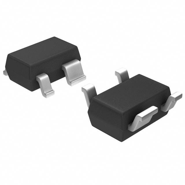
3
4
2
1
SOT343
Applications
• LNA for GSM, GPS, DCS, PCS, UMTS, Bluethooth, ISM and WLAN
9FF��
,Q��
2XW��
2Q�2II
���N2KP
*1'��
%*$���B3LQBFRQQHFWLRQ�YVG
Figure 1
Pin connection
Description
The BGA622 is a wide band low noise amplifier, based on Infineon Technologies’ Silicon Germanium Technology
B7HF. In order to provide the LNA in a small package the out-pin is simultaneously used for RF out and On/Off
switch. This functionality can be accessed using a RF-Choke at the Out pin, where a DC level of 0 V or an open
switches the device on and a DC level of VCC switches the device off. While the device is switched off, it provides
an insertion loss of 24 dB together with a high IIP3 up to 20 dBm.
Type
Package
Marking
BGA622
SOT343
BXs
Note: ESD: Electrostatic discharge sensitive device, observe handling precaution
Data Sheet
4
Rev. 2.2, 2008-04-14
�BGA622
Silicon Germanium Wide Band Low Noise Amplifier with 2 kV ESD Protection
Maximum Ratings
Table 1
Maximum ratings
Parameter
Symbol
Limit Value
Unit
Voltage at pin VCC
VCC
Vout
Iin
Iout
IVcc
Pin
Ptot
TJ
TA
TSTG
VESD
3.5
V
4
V
0.1
mA
1
mA
10
mA
6
dBm
35
mW
150
°C
-65... 150
°C
-65... 150
°C
2000
V
Voltage at pin Out
Current into pin In
Current into pin Out
Current into pin VCC
RF input power
Total power dissipation, TS < 139 °C
1)
Junction temperature
Ambient temperature range
Storage temperature range
ESD capability all pins (HBM: JESD22-A114)
1) TS is measured on the ground lead at the soldering point
Note: All Voltages refer to GND-Node
Thermal resistance
Table 2
Parameter
Thermal resistance
Value
Unit
RthJS
300
Junction - soldering point1)
1) For calculation of RthJA please refer to Application Note Thermal Resistance
K/W
Data Sheet
Symbol
5
Rev. 2.2, 2008-04-14
�BGA622
Electrical Characteristics
2
Electrical Characteristics
2.1
Electrical characteristics at TA = 25 °C (measured according to Figure 2)
VCC = 2.75 V, Frequency = 1.575 GHz, unless otherwise specified
Table 3
Electrical Characteristics
Parameter
Symbol
Values
Insertion power gain
|S21|2
|S21|2
RLin
RLout
F50Ω
IIP3
15.0
dB
-27
dB
5
dB
12
dB
1.00
dB
0
dBm
IIP3
20
dBm
-16.5
dBm
Min.
Insertion power gain (Off-State)
Input return loss (On-State)
Output return loss (On-State)
Noise figure (ZS = 50 Ω)
Input third order intercept point
(On-State)
1)
Input third order intercept point1)
(Off - State)
Typ.
Input power at 1 dB gain compression P-1dB
Unit
Max.
Total device off current
Itot-off
130
260
420
µA
Total device on current
Itot-on
Von
4.0
5.8
7.8
mA
0.8
V
On / Off switch control voltage
0
Note /
Test Condition
f = 0.1 GHz
∆f = 1 MHz,
PIN = -28 dBm
∆f = 1 MHz,
PIN = -8 dBm
VCC = 2.75 V,
Vout = VCC
VCC = 2.75 V
VCC = 2.75 V
ON-Mode:
Vout = Von
Voff
2.0
3.5
V
VCC = 2.75 V
OFF-Mode:
Vout = Voff
1) IP3 values depends on termination of all intermodulation frequency components. Termination used for this measurement
is 50 Ω from 0.1 to 6 GHz
Data Sheet
6
Rev. 2.2, 2008-04-14
�BGA622
Electrical Characteristics
2.2
Electrical characteristics at TA = 25 °C (measured according to Figure 2)
VCC = 2.75 V, Frequency = 2.14 GHz, unless otherwise specified
Table 4
Electrical Characteristics
Parameter
Symbol
Values
Min.
Insertion power gain
Insertion power gain (Off-State)
Input return loss (On-State)
Output return loss (On-State)
Noise figure (ZS = 50 Ω)
Input third order intercept Point
(On-State)
Typ.
2
1)
Input third order intercept point1)
(Off-State)
Unit
Max.
Note /
Test Condition
|S21|
|S21|2
RLin
RLout
F50Ω
IIP3
13.6
dB
-24
dB
7
dB
10
dB
1.05
dB
3
dBm
∆f = 1 MHz,
PIN = -28 dBm
IIP3
20
dBm
∆f = 1 MHz,
PIN = -8 dBm
Input power at 1 dB gain compression P-1dB
-13
dBm
1) IP3 values depends on termination of all intermodulation frequency components. Termination used for this measurement
is 50 Ω from 0.1 to 6 GHz
DC,
2.75V
Out, 50 Ω
150pF
In, 50 Ω
BGA622_S_Parameter_Circuit.vsd
Figure 2
Data Sheet
S-Parameter Test Circuit (loss-free microstrip test-fixture)
7
Rev. 2.2, 2008-04-14
�BGA622
Electrical Characteristics
DC,
2.75V
Out
47pF (DC-Block)
RFC
150pF
On/Off
Switch
DC,
2.75V
2.2nH (for improved input match)
47pF (DC-Block)
In
BGA622_Application_Circuit.vsd
Figure 3
Data Sheet
Application Circuit for 1800 - 2500 MHz
8
Rev. 2.2, 2008-04-14
�BGA622
Measured Parameters
3
Measured Parameters
2
2
Power Gain |S | , G = f(f)
21
ma
V = 2.75V, I
= 5.8mA
CC
Off Gain |S | = f(f)
21
V = 2.75V, V
= 2.75V, I
tot−on
CC
25
OUT
tot−off
= 0.3mA
0
−5
G
ma
−10
−15
|S21|2
15
−20
2
|S21| [dB]
|S21|2, Gma [dB]
20
−25
10
−30
−35
5
−40
0
−45
0
1
2
3
4
5
6
0
1
Frequency [GHz]
Reverse Isolation |S | = f(f)
12
= 5.8mA
V = 2.75V, I
CC
2
3
4
5
6
5
6
Frequency [GHz]
Matching |S |, |S | = f(f)
11
22
= 5.8mA
V = 2.75V, I
tot−on
CC
tot−on
0
0
−5
−2
S11
−4
−10
−6
|S11|, |S22| [dB]
|S12| [dB]
−15
−20
−25
−8
−10
−12
−30
−14
−35
−16
−40
−18
S22
−45
−20
0
1
2
3
4
5
6
0
Frequency [GHz]
Data Sheet
1
2
3
4
Frequency [GHz]
9
Rev. 2.2, 2008-04-14
�BGA622
Measured Parameters
Stability K, B = f(f)
1
VCC = 2.75V, I tot−on = 5.8mA
Noise Figure F = f(f)
VCC = 2.75V, I tot−on = 5.8mA, ZS = 50Ω
5
1.5
4.5
1.4
4
1.3
3.5
1.2
3
1.1
F [dB]
K, B1
K
2.5
2
1
0.9
1.5
0.8
B1
1
0.7
0.5
0.6
0
0.5
0
1
2
3
4
5
6
0
0.5
Frequency [GHz]
1
1.5
2
2.5
3
Frequency [GHz]
Input Compression Point P
= f(V )
−1dB
CC
f = 2.14GHz, T = parameter in °C
Device Current I
= f(T , V )
tot−on
A CC
V
=
parameter
in
V
CC
A
−10.5
8.5
85
3.4
−11
8
20
−11.5
7.5
Itot−on [mA]
P−1dB [dBm]
−40
−12
−12.5
3.2
7
3
6.5
2.8
−13
6
−13.5
5.5
2.6
−14
2.6
2.8
3
3.2
5
−40
3.4
VCC [V]
Data Sheet
−20
0
20
40
60
80
TA [°C]
10
Rev. 2.2, 2008-04-14
�BGA622
Measured Parameters
Power Gain |S |2 = f(T , V )
21
A CC
f = 2.14GHz, V
= parameter in V
Device Current I
= f(V , T )
tot−on
CC
A
T A = parameter in °C
CC
8.5
15
−40
8
14.5
20
7.5
14
7
|S |2 [dB]
3.4
21
Itot−on [mA]
85
6.5
13.5
3
6
13
5.5
2.6
5
2.6
2.8
3
V
CC
3.2
12.5
−40
3.4
[V]
−20
0
20
40
60
80
T [°C]
A
2
Power Gain |S | = f(V , T )
21
CC
A
f = 2.14GHz, T = parameter in °C
A
15.5
15
−40
|S21|2 [dB]
14.5
14
20
13.5
85
13
12.5
2.6
2.8
3
3.2
3.4
VCC [V]
Data Sheet
11
Rev. 2.2, 2008-04-14
�BGA622
Package Information
4
Package Information
2 ±0.2
0.9 ±0.1
B
1.3 ±0.1
0.20
0.1 max
B
M
0.3
1
2
+0.2
acc. to
DIN 6784
2.1±0.1
3
1.25 ±0.1
A
4
0.15 +0.1
-0.05
+0.1
0.6 +0.1
0.20
M
A
GPS05605
Figure 4
Package Outline SOT343
0.2
2.3
8
4
Pin 1
Figure 5
Data Sheet
2.15
1.1
Tape for SOT343
12
Rev. 2.2, 2008-04-14
�